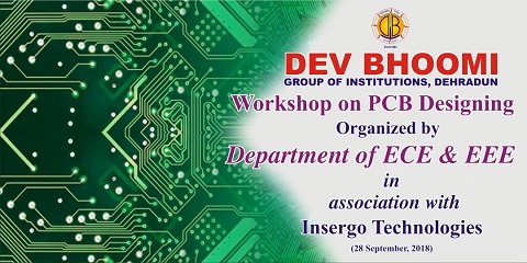
Workshop on PCB designing By ECE & EEE Department
ABOUT EVENT

WORKSHOP ON PCB DESIGNING
ORGANISED BY DEPARTMENT OF ECE & EEE IN ASSOCIATION WITH INSERGO TECHNOLOGIES
Dated 28th September 2018
The objective of this workshop is to make the students familiar with basic steps of designing the PCB layouts of the electronic & electrical circuits through DIP-TRACE Software
A printed circuit board (PCB) mechanically supports and electrically connects electronic components using conductive tracks, pads, and other features etched from copper sheets laminated onto a non-conductive substrate. A printed circuit board has pre-designed copper tracks on a conducting sheet. Dip-Trace is quality Schematic Capture and PCB Design software that offers everything to create simple or complex multi-layer boards from schematic to manufacturing files. PCB Layout is a high-level engineering tool for board design featuring smart manual routing of high-speed and differential signals, shape-based auto router, advanced verification, and wide import/export capabilities. Dip-Trace features design process with real-time DRC, which reports errors on the fly before actually making them. The board can be previewed in 3D and exported for mechanical CAD modeling.
